Reprogramming becomes impossible to small PIC !
 |
| The yellow LED on the JDM Programmer blinked. PIC16F819 was supplied power from the JDM Programmer. |
|
| The yellow LED on the JDM Programmer blinked. PIC16F819 was supplied power from the JDM Programmer. |
The JDM programmer is a very useful programmer. However, when powerful PIC appeared in small size, one difficult problem was raised. It is the problem that reprogramming after next time will become impossible, when "CONFIG" is set to both "IntOSC" and "MCLR OFF."
Shigerunosuke raised this problem for the first time on the forum of Japan about the JDM programmer.
Although I did not believe suddenly, when experimented using PIC12F675, the result became the same as the problem which Mr. Shigerunosuke raised.(Note) A result changes with a program code. It does not necessarily surely become so on any conditions.
It also became impossible to erasing PIC12F675 of me from next time.
I thought whether PIC12F675 of me would have broken.
Then, I investigated anew about the sequence that enters the device into the Programming/Verify mode. And I understood the following thing.
The Program/Verify mode is entered by holding pins CLOCK and DATA low while raising MCLR pin from VIL to VIHH (high voltage). Apply VDD and data. Once in this mode, the user program memory, data memory and the configuration memory can be accessed and programmed in serial fashion.
The MCLR pin must be raised from VIL to VIHH before VDD is applied. This is to ensure that the device does not have the PC incremented while in valid operation range.
Do not power GP2, GP4 or GP5 before VDD is applied.
The JDM programmer always supplies power to the device, and cannot control VDD.
Therefore, power is supplied on a JDM programmer to PIC, and it excutes the program code already written in it.
I tried also using PIC16F819.
CONFIG was set as "IntOSC" and "MCLR OFF", and the program code which blinks LED was written in.
After programming was completed, JDM programmer's LED started blink.
It was set to evaluation board in order to confirm whether the program is normally written in PIC16F819.
Four LEDs on the evaluation board blinked. The PIC is working well.
But, next time to reprogramming was impossible using the JDM programmer.
Shiro suggested the solution of this problem to me. He said that what is necessary was just to make it Vdd turned on, when Vpp carried out turn-on using the transistor. Then, I tried the solution which he suggested using two transistors. The result was good.
Similarly, the addition circuit using two transistors was contributed to the forum of IC-Prog by HOGEPIYOHAMU. HOGEPIYOHAMU's Page
Next, I added the delay circuit of Vdd using a photo-coupler to the JDM programmer.
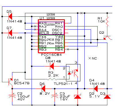
Ebihara also devised another delay circuit using one PNP transistor. Ebi-memo
Aram Mine built an adapter based on the above-mentioned circuit, and enabled it to use it on a JDM programmer. Circuit diagram
Furthermore, there is another solution by BT Kelly. JDM Programmer Modification
It is thought that all of the above-mentioned solution are effective in 12F629 or 12F675. It seems that but OSCCAL may be lost under a certain conditions. Or programming to the devices of 18- pin occasionally goes wrong. Then, I decided to devise "RCD programmer."
Note(added 2006-02-18)
PIC12C508/508A/CE518, PIC12C509/509A/CE519
Apply Vpp first
Because the memory type of these devices is "OTP", these devices cannot be erased and cannot be programmed again.
JDM Programmer can program these devices well, but can not read/verify when configuration word is set to both "Internal RC oscillator" and "MCLR internally connected to VDD"
The following is the quotation from "PIC12C5XX Memory Programming ".
The MCLR pin should be raised from VIL to VIHH within 9 ms of VDD rise.
This is to ensure that the device does not have the PC incremented
while in valid operation range.
PIC12F508/509
Apply Vdd first
JDM Programmer can program these devices well, but can not read/verify/erase when configuration word is set to both "Internal RC oscillator" and "MCLR internally tied to VDD"
The following is the quotation from "PIC12F508/509 Memory Programming Specification".
The Program/Verify mode is entered by holding pins
ICSPCLK and ICSPDAT low while raising VDD pin from
VIL to VDD. Then raise VPP from VIL to VIHH.
PIC12F629/675, PIC16F630/676
Apply Vpp first
JDM Programmer can program these devices well, but can not read/verify/erase when configuration word is set to both "INTOSC oscillator" and "MCLR function is internally disabled"
The following is the quotation from "PIC12F629/675/PIC16F630/676 Memory Programming".
The Program/Verify mode is entered by holding pins clock
and data low while raising MCLR pin from VIL to VIHH
(high voltage). Apply VDD and data.
PIC12F635/683, PIC16F636/639, PIC16F684/688, PIC16F685/687/689/690
Apply Vpp first and Apply Vdd first two-way
JDM Programmer can program these devices well, but can not read/verify/erase when configuration word is set to both "INTOSC oscillator" and "MCLR function is internally disabled".
The following is the quotation from revised "PIC12F6XX/16F6XX Memory Programming Specification".
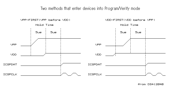
3.0 PROGRAM/VERIFY MODE
Two methods are available to enter Program/Verify
mode. The “VPP-first” is entered by holding ICSPDAT
and ICSPCLK low while raising MCLR pin from VIL to
VIHH (high voltage), then applying VDD and data. This
method can be used for any configuration word
selection and must be used if the INTOSC and internal
MCLR options are selected (FOSC<2:0> = 100 or 101
and MCLRE = 0). The VPP-first entry prevents the
device from executing code prior to entering Program/
Verify mode. See the timing diagram in Figure 3-1.
The second entry method, “VDD-first”, is entered by
applying VDD, holding ICSPDAT and ICSPCLK low,
then raising MCLR pin from VIL to VIHH (high voltage),
followed by data. This method can be used for any
configuration word selection except when INTOSC
and internal MCLR options are selected
(FOSC<2:0> = 100 or 101 and MCLRE = 0). This
technique is useful when programming the device
when VDD is already applied, for it is not necessary to
disconnect VDD to enter Program/Verify mode. See the
timing diagram in Figure 3-2.
Once in this mode, the program memory, data memory,
and configuration memory can be accessed and
programmed in serial fashion. ICSPDAT and ICSPCLK
are Schmitt Trigger inputs in this mode. RA4 is tristate,
regardless of fuse setting.
The sequence that enters the device into the Programming/
Verify mode places all other logic into the Reset
state (the MCLR pin was initially at VIL). Therefore, all
I/O’s are in the Reset state (hi-impedance inputs) and
the Program Counter (PC) is cleared.
To prevent a device configured with INTOSC and
internal MCLR from executing after exiting Program/
Verify mode; VDD needs to power-down before VPP.
modified: 2006-2-18 JST
2004-3-11 JST